Empowering the next generation of silicon innovation with precision-driven VLSI expertise, advanced node design, and high-performance verification.
Advanced circuit design and simulation leveraging industry-standard Electronic Design Automation (EDA) tools to deliver high-precision silicon verification. Our ESDM services cover the complete semiconductor lifecycle, ensuring accuracy, scalability, and performance from concept to fabrication.

End-to-end design flow using Cadence Virtuoso and Innovus tools, delivering robust analog, digital, and mixed-signal verification with industry best practices.

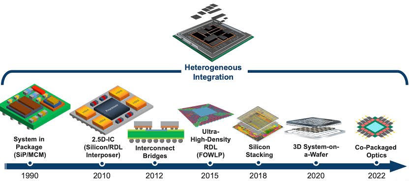
The semiconductor chip design industry is a high-value, complex sector focused on creating integrated circuit blueprints, crucial for AI, data centers, EVs, and IoT. With major global players and growing R&D investment in India, driven by advanced computing demand and government initiatives like ISM, the industry relies on sophisticated EDA tools for ASIC and FPGA design while pushing toward smaller nodes (3nm+) for higher performance.


Holistic system-level architectural integration and multi-core synchronization.

Seamless merging of custom IPs and standard protocol controllers.

Optimizing Network-on-Chip (NoC) and AMBA bus protocols.
Advanced multi-voltage domain management for low-power designs.
Developing ultra-low power silicon designed specifically for the massive scale and connectivity requirements of the IoT ecosystem.

On-chip wireless protocols including BLE, WiFi 6, and Zigbee.

Sub-threshold design techniques for decade-long battery life.

Designing high-throughput neural processing units (NPUs) and tensor engines for edge and data center artificial intelligence.

Specialized datapath architectures for matrix multiplication operations.
Maximizing TOPS/Watt for battery-constrained AI inference applications.